
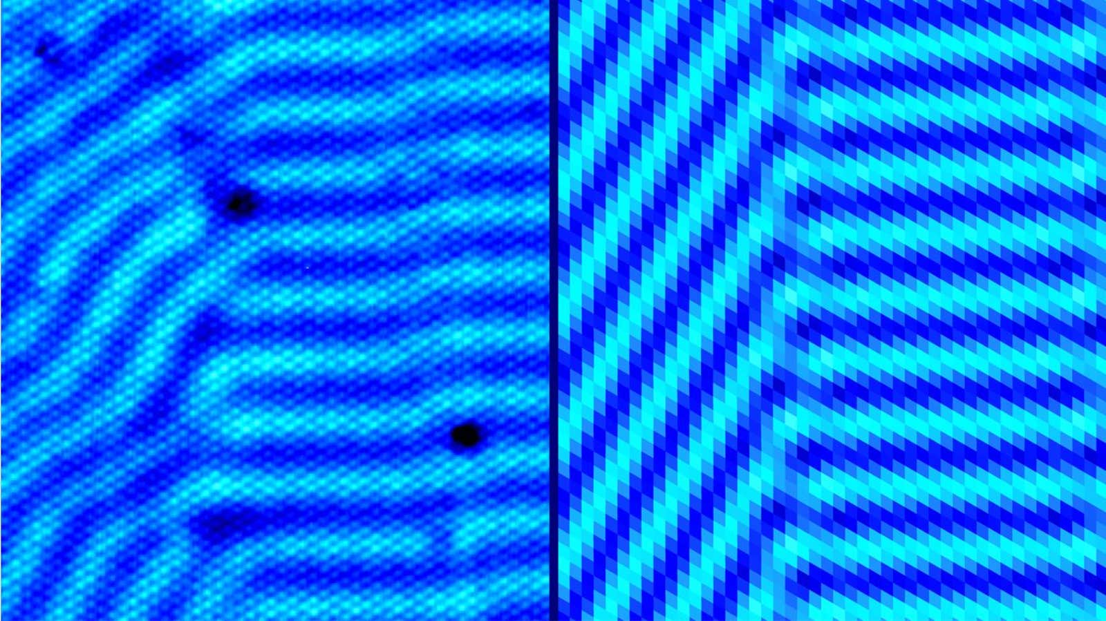

The stripes looked like a mistake.
Several years ago, a team of physicists at Stanford University led by Aharon Kapitulnik was trying to grow a thin layer of bismuth crystal on a metallic surface. But instead of forming a uniform sheet, the crystal became a patchwork of uneven growth. In some areas—those where the crystal layer was only one atom thick—a striking design emerged. Small stripes filled up irregular patches, and these regions butted against one another, their stripes oriented at different angles.
Kapitulnik couldn’t explain the stripes. Then on a working trip to Paris in 2017, he showed them to Yuki Fuseya, a theorist at the University of Electro-Communications in Chofu, Japan. “This is like a zebra,” Fuseya told Kapitulnik. And if the stripes were really like a zebra’s, he said, they could be a Turing pattern.
The possibility came as a surprise. Countless patterns in nature, from zebra stripes to psychedelic hallucinations and windswept ripples in sand, are thought to stem from a mechanism that Alan Turing proposed in 1952, between his famed code-breaking work during World War II and his tragic death in 1954. This kind of pattern has since been identified in the arrangement of bacteria, stripes on sea shells, and even the distribution of human settlements. This ever-growing list includes systems on vastly different scales, from embryos to galaxies.
But bismuth sheets seemed to be missing some of the Turing patterns’ essential ingredients. Turing’s paper described a theoretical mechanism based on two substances—an activator and an inhibitor that diffuse across an area at different rates. The interaction between these two “morphogens,” as Turing called them, allows one to interrupt the effect of the other—creating a pattern of colored lines on a tropical fish, for example, rather than a solid color.
But in the case of the bismuth crystal, there is no diffusion. Molecules don’t shift randomly and spread out while reacting with each other. Nevertheless, Fuseya, Kapitulnik and several collaborators began to simulate bismuth crystal growth using Turing’s equations. After three years, they ended up with a simulated pattern, published July 2021 in Nature Physics, that looked almost identical to the stripes in the real crystal. “It was really an amazing match,” Kapitulnik said. It convinced him that Turing’s mechanism was indeed responsible for the stripes in the bismuth. And it demonstrated once again how robust and powerful Turing’s original insight was.
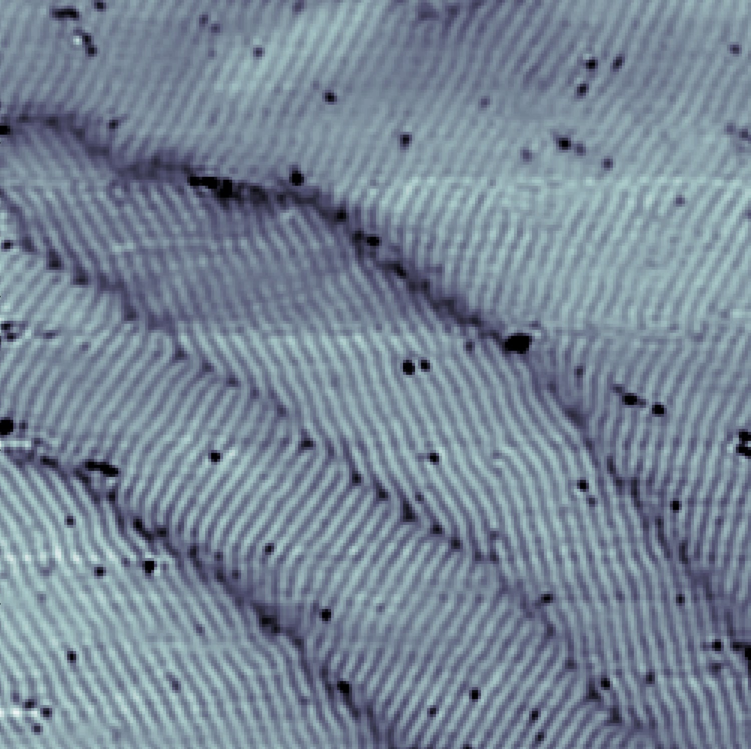
Here, the stripe-forming process is driven by the forces at play among the bismuth atoms and the metal below. Bismuth atoms want to fit into particular spots on the molecular lattice of the metal. But these spots are closer together than the bismuth atoms find comfortable. Like a photograph that gets shoved into a frame that’s too small for it, the sheet of bismuth atoms buckles. The strain creates a wavy pattern that leaves some atoms raised, forming the stripes. The vertical shift—movement away from the plane of the crystal—acts as the activator in the Turing equations, while the shift within the plane acts as the inhibitor. The morphogens here are displacements, not molecules.
The researchers were not the first to use untraditional variables in their Turing equations. According to Andrew Krause, a mathematician at the University of Oxford, scientists have modeled Turing patterns in the interactions of predators and prey, while others have used whole cells as variables. But he’s never seen a model using displacement before.
Though the bismuth didn’t diffuse or react the way Turing imagined, the paper demonstrated that the crystal showed the same behavior as a Turing pattern, said Irving Epstein, a chemist at Brandeis University. “The more I read it, actually, the more I liked it,” he said. The findings suggest that this version of Turing’s pattern-formation mechanism might crop up in more systems than scientists have typically considered.
The bismuth stripes contrast with other Turing patterns in another way: They are tiny, each about 1 nanometer wide, or 10 millionths of the width of a human hair. “The scale is very important here,” Epstein said. “The fact that you’re seeing these patterns on a scale that’s a million times smaller than the kinds of distances that one sees in chemical and biological patterns I think is impressive.”
Turing’s equations may govern the small-scale growth of other crystals as well. Since publishing the work, Fuseya says he has heard from scientists who are identifying Turing patterns in their own materials. “Experimentalists already see that pattern, but they never realized that this is the same mechanism as in tropical fish,” he said. “I expect that in other materials we will see the same properties.”
The properties of Turing patterns include more than just their form. When part of a Turing pattern is wiped out, it grows back. You might not assume that inorganic materials like bismuth crystals would be able to heal as animals do, Fuseya said, but indeed, his team’s simulated bismuth crystal was able to mend itself. Kapitulnik hasn’t tested real bismuth yet, but the robustness of the crystal growth and the way neighboring regions met and grew together suggested to him that the material would be able to fix interruptions in the pattern.
The researchers noted that the new knowledge gleaned from bismuth may come in handy in the engineering of microdevices, which require microscopic components. Kapitulnik is especially interested in testing for this pattern in materials such as tin, which is widely used in superconductors. And if the same mechanism applies to other materials on the atomic scale, then it could reveal how to manipulate crystal growth. “Often that kind of technique development can then percolate and become something totally different,” Krause said.
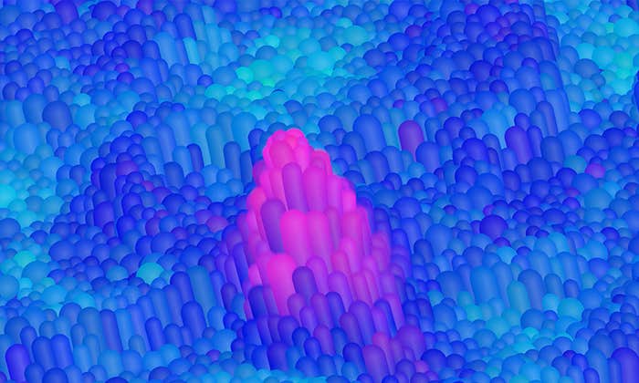
Lead image: The nanometer-wide stripes seen in crystal growth (left) closely match those formed in a theoretical model based on Turing patterns (right). Credit: Alan Fang & Aharon Kapitulnik; Yuki Fuseya